Create New Job
Click Start Job

Layout Options
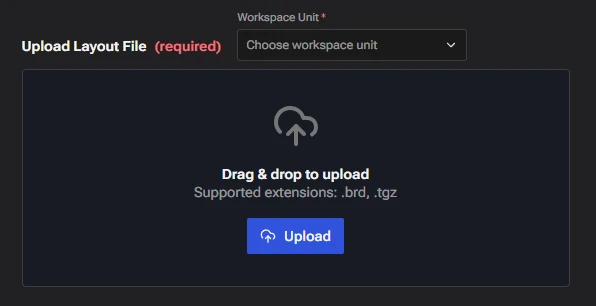
Workspace Unit
By default, the tool should consider millimeters (MM) as the unit during simulation and report generation. Currently, the tool supports millimeters.
Upload Design
Under the Upload Layout File section, upload your layout file with a supported file extension. The currently supported file types are ODB++ (.tgz) and Allegro Board (.brd).
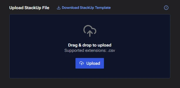
Upload StackUp
Under the Upload StackUp File section, upload your StackUp file to update the design StackUp. The supported format for the StackUp file is .csv.
Why is the StackUp file used?
To calculate the impedance of a single-ended trace or the differential impedance of a differential pair of traces.
- Make sure the StackUp unit is the same as the one you selected.
- The name of the StackUp file should be layers.csv.
- Below is the snapshot of the StackUp file and a brief description of the format and layers information to be filled.
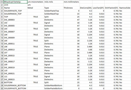
About StackUp
- All lines starting with “#” are commented lines.
- In the row “Unit”, enter the unit type. Currently supported unit types are mm, mils, and um.
- In the column “Name”, enter the name of the layer as you want for a clear understanding of the layer numbers.
- In the column “Metal”, enter “TRUE” for all the metal layers like Signal, Split, or Plane.
- In the column “Type”, enter “Signal” for signal layers, “Plane” for solid plane layers, and “Split” for layers that have both signal and solid plane. For all the dielectric layers, enter “Dielectric”.
- In the column “Thickness”, enter the thickness of the respective layers based on the unit type of the StackUp.
- In the “DieCons(DK)” column, enter the value of the dielectric constant for each layer.
- In the “LossTan(DF)” column, enter the value of the loss tangent for each layer.
- Enter the etch factor (if applicable) in the “EtchFactor(EF)” column for each layer.
- Enter “No” for all the layers in the “NarrowSide” column.
Target Chips
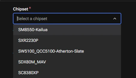
Choose Chipset
From the drop-down menu under the Compute → Chipset section, select the chipset of interest.
Choose Technology Area
From the drop-down menu under the Compute → Technology section, select MSM.

Choose Target Chip
From the drop-down menu under the Compute → Target Chip section, select MSM.

Choose Interface
From the drop-down menu under the Compute → Interface section, select the interface for which you want to submit the job.
You can select multiple interfaces at a time, and an unique Job ID will be created for each interface.
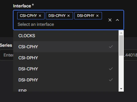
Why choose an interface?
Different interfaces of a chipset have different sets of electrical nets and require different sets of rules to be executed due to design guideline differences. Therefore, interface selection is important to perform the electrical DRC (Design Rule Check) of a given chipset.
Enter Refdes
For each interface selected in the previous step, enter the respective refDes value in the designated section. The refDes is required to validate pins in the OL CSV file using the refDes pins. It's also used to obtain connected Electrical Nets from the refDes pins in order to execute the rules.
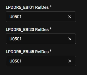
NOTE
The RefDes name for all selected interfaces must be identical.
Project information
- Enter the project name in the Project Name* section.
- Enter the OEM or Target Equipment in the OEM/Target Equipment* section.
- If you have any notes, enter them in the Notes section for your reference.
- If required, enter the email ID of the person in the CC Result to Users section to send an email notification upon job completion. You can enter multiple email IDs, separated by commas.
NOTE
To receive an email notification after job completion, make sure to check the Notify by Email box.
The design must be 100% uploaded before you can submit the job. If the design is not fully uploaded, the Submit Job button will remain disabled.