Create New Job
Click Start Job

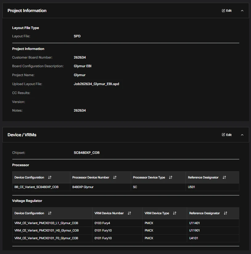
Job Submission Overview
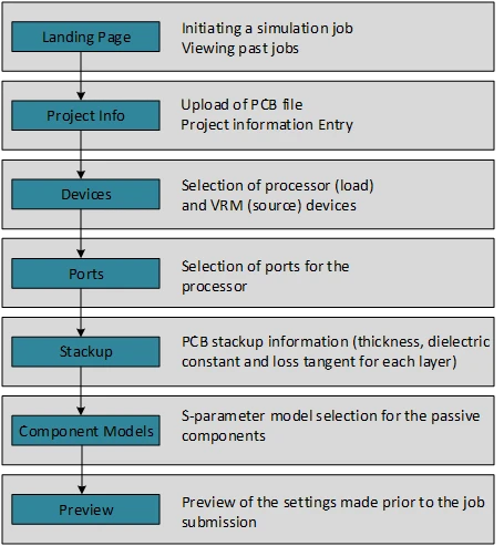
Layout File & Project Information
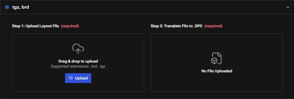
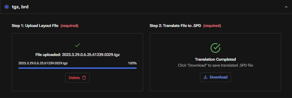
Upload the PCB file. ODB++, Cadence .BRD and Cadence .SPD files are supported. If you are selecting ODB++ or .BRD file, you will need to upload and then translate to .SPD.
Upload brd file & translate
Upload Spd file

Project information
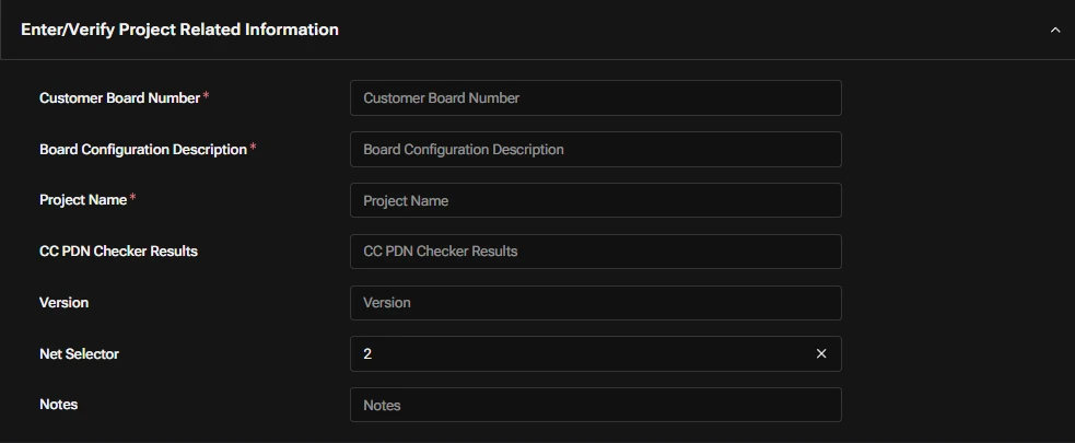
- Customer Board Number: Enter any identification number for the PCB. This is for your tracking purpose.
- Board Configuration Description: Enter a name for the presets. The settings you configure in this simulation job will be stored with that name. This name can be used to recall the settings in future versions of the tool.
- Project Name: Enter name of the project. This is for your tracking purpose.
- If required, enter the email ID of the person in the CC Result to Users section to send an email notification upon job completion. You can enter multiple email IDs, separated by commas.
- Version: Enter version number of the PCB (Optional). This is for your tracking purpose.
- Net Selector: If there are series components on the rails, such as a 4-terminal resistor for current sensing, change the net selector value to the number of terminals of the series component.
- Notes: Use this space to include notes about the changes made to the PCB (optional). This is for your tracking purposes.
The design must be 100% uploaded before you can submit the job. If the design is not fully uploaded, the Submit Job button will remain disabled.
Device Selection
Choose Chipset and Configuration
Select the applicable chipset. It will automatically load the SoC and associated PMICs for the Core, SERDES and memory EBI simulations.
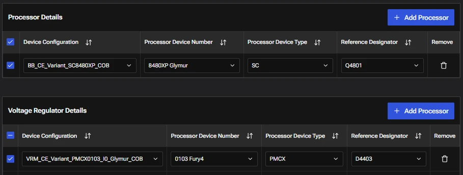
Choose Processors and Vrms
- Processors (loads) are listed here. Enable appropriate row for the processor, if there are more than one processor listed. Select the reference designator for the processor.
- Voltage Regulator Modules (VRMs) (source) are listed here. Set the reference designators for each VRM. These devices are necessary to report the DCR numbers.
Select Ports
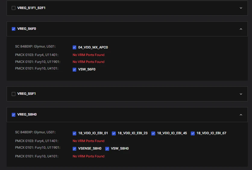
- You can select all the ports by clicking on the Select/Deselect All checkbox, Ports (from load and source) are listed based on the selection made in the previous step.
- You can individually enable/disable the PDN rails, this is useful to quickly get the results for only those rails which are modified in the layout.
- Ports which are associated with the rails are listed here, You can partially enable the ports on the source side.
- You can deselect certain VRM ports. This option is useful to get the DCR between the load and a particular source if there are multiple sources. However, recommended to keep it at default (all enabled).
StackUp Information
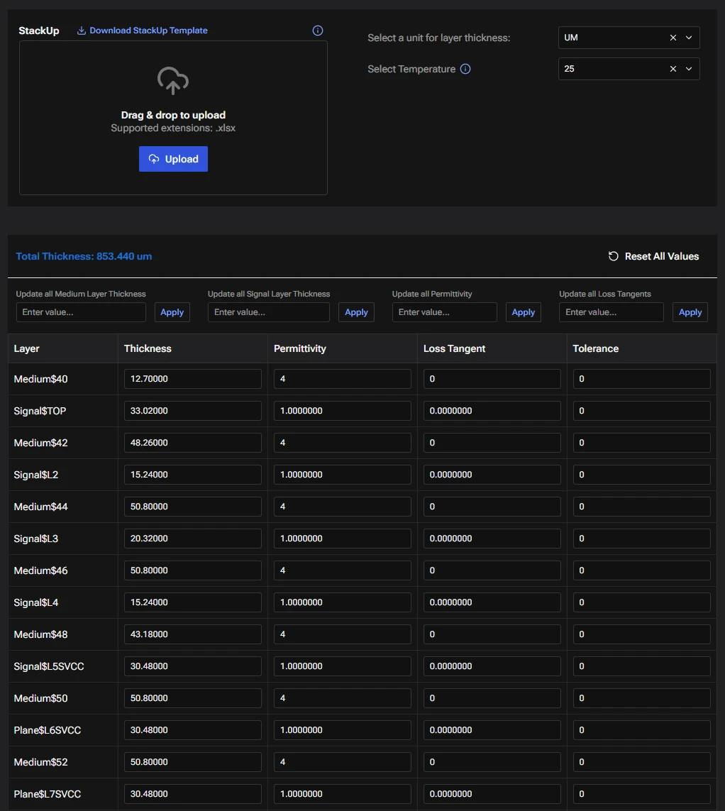
- The table provides information about the layer thickness, dielectric constant, and loss tangent from the uploaded PCB. If you wish to modify the data, you can edit it manually in the table or download the template spreadsheet and upload it back after updating the values. Please do not modify the layer names or add any layers in the template file; the layer information is obtained from the uploaded PCB itself.
- Select the temperature.
NOTE
Conductivity of copper is adjusted based on the selected temperature.
- You can update parameters for all layers at once with the same value.
- Click on reset to load the table values from the uploaded PCB.
Select Component Models
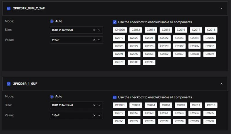
- Part names of the passive components (shunt and series elements) connected to the rails under simulation are shown. Click on the checkbox to start assigning the models.
NOTE
Default capacitor vendor models will be used. All the components should be modelled except any active devices (including load and source), test points, connectors and other loads which are not expected to impact the PDN simulation results.
- You need to select the Size and Value parameter. For example: 0201 (Size) 1uF (Value).
- You can DNI (do not install) the components by clicking on the reference designators shown under each part name.
Preview
This page allows you to review the settings configured for the simulation job. Once verified, you can click the Submit Job button to start the simulation. If you want to make any changes to the settings, you can click the Prev/Edit button.
